DIL/NetPC DNP/1486
In-deep Contact us
Sales
Support
Back to Top Page
DIL/NetPC DNP/1486-3V: Parts and Components
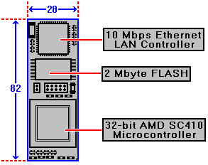
A DIL/NetPC DNP/1486-3V is based on a 8-level multilayer printed circuit board (PCB). On this PCB with the size of only 82mm * 28mm are assembled numerous different components with SMD technology. Thereby both sides of the PCB are used for mounting the SMD components. The following figure shows the position of the most important components on the upper side of the DNP/1486-3V PCB.

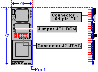
The central component on the printed circuit board upper side forms the 32-bits low power AMD SC410 microprocessor. Close to the SC410 is found a 2 Mbyte FLASH memory chip with the entire firmware (BIOS, operating system, TCP/IP stack and application programs) as well as a 10 Mbps 10BASE-T Ethernet LAN controller with embedded buffer memory. Furthermore there are the 2-pin jumper JP1 and the 10-pin connector J2 available.

The jumper JP1 activates or deactivates the REMOTE CONSOLE MODE (RCM) function of the DIL/NetPC DNP/1486-3V. In this mode a user can operate the DIL/NetPC with a external PC and a terminal emulation program (for example Microsoft Windows HyperTerminal). The terminal program will be the "remote console" for the DIL/NetPC. If the RCM activated the console output, including the boot messages, are given out to the DIL/NetPC COM1 port. Console inputs goes the same way to COM1.
DNP/1486-3V Jumpers and Connectors
Name
Function
JP1
Jumper. REMOTE CONSOLE MODE RCM) ON / OFF.
J1
Connector. 64-pin DIL Pinout.
J2
Connector. JTAG Interface for Factory- Test and Setup.
If the REMOTE CONSOLE MODE is activ (jumperposition JP1 closed = RCM activ), the DIL/NetPC is given out all boot messages from the BIOS and the operating system to the COM1 port. It is not examined, whether a PC with a terminal emulation program is connected to this port. Thereby is the COM1 port only for test and diagnostic suitable. The REMOTE CONSOLE MODE should be used only in the development stage. After that the jumper can be pulled (jumperposition JP1 open for "RCM not activ"). The REMOTE CONSOLE MODE is then not activ. In this condition no console I/O goes over the DIL/NetPC COM1 port. This port is then free for use by a application software.
Function of Jumper JP1 (REMOTE CONSOLE MODE)
JP1
Function
Jumperposition closed (Default Factory Setup)
REMOTE CONSOLE MODE ON (activ)
Jumperposition open
REMOTE CONSOLE MODE OFF (not activ)
It is to be considered, that the DIL/NetPC DNP/1486-3V examines the jumper JP1 only in the boot phase. Thus you should change these jumper only in the power off condition.
The connector J1 is formed through the 64-pin JEDEC DIL (dual-in-line) pinout. Please note, that the Pin 1 is marked for the DIL pinout on the upper side of the DIL/NetPC DNP/1486-3V printed circuit board. The connector J2 serves exclusively for the production and factory setup of the DIL/NetPC DNP/1486-3V. The pinout and function of this JTAG interface can change any time without announcement. If you need this pinout please contact the DIL/NetPC product support. Connector J2 is joined directly with the JTAG interface of the AMD SC410 microprocessor. In the factory setup we use this connector for programming the first boot loader to the DIL/NetPC FLASH memory chip. We also use J2 for the product test.
J1 64-pin DIL Connector Pinout
Pin
Name
Function
Direction
1
PA0
Parallel I/O, Port A, Bit 0
IN/OUT
2
PA1
Parallel I/O, Port A, Bit 1
IN/OUT
3
PA2
Parallel I/O, Port A, Bit 2
IN/OUT
4
PA3
Parallel I/O, Port A, Bit 3
IN/OUT
5
PA4
Parallel I/O, Port A, Bit 4
IN/OUT
6
PA5
Parallel I/O, Port A, Bit 5
IN/OUT
7
PA6
Parallel I/O, Port A, Bit 6
IN/OUT
8
PA7
Parallel I/O, Port A, Bit 7
IN/OUT
9
PB0
Parallel I/O, Port B, Bit 0
IN/OUT
10
PB1
Parallel I/O, Port B, Bit 1
IN/OUT
11
PB2
Parallel I/O, Port B, Bit 2
IN/OUT
12
PB3
Parallel I/O, Port B, Bit 3
IN/OUT
13
PB4
Parallel I/O, Port B, Bit 4
IN/OUT
14
PB5
Parallel I/O, Port B, Bit 5
IN/OUT
15
PB6
Parallel I/O, Port B, Bit 6
IN/OUT
16
PB7
Parallel I/O, Port B, Bit 7
IN/OUT
17
PC0
Parallel I/O, Port C, Bit 0
IN/OUT
18
PC1
Parallel I/O, Port C, Bit 1
IN/OUT
19
PC2
Parallel I/O, Port C, Bit 2
IN/OUT
20
PC3
Parallel I/O, Port C, Bit 3
IN/OUT
21
RXD
COM1 Serial Port, RXD Pin
IN
22
TXD
COM1 Serial Port, TXD Pin
OUT
23
CTS
COM1 Serial Port, CTS Pin
IN
24
RTS
COM1 Serial Port, RTS Pin
OUT
25
DCD
COM1 Serial Port, DCD Pin
IN
26
DSR
COM1 Serial Port, DSR Pin
IN
27
DTR
COM1 Serial Port, DTR Pin
OUT
28
RI
COM1 Serial Port, RI Pin
IN
29
RESIN
RESET Input
IN
30
TX+
10BASE-T Ethernet Interface, TX+ Pin
OUT
31
TX-
10BASE-T Ethernet Interface, TX- Pin
OUT
32
GND
Ground
----
33
RX+
10BASE-T Ethernet Interface, RX+ Pin
IN
34
RX-
10BASE-T Ethernet Interface, RX- Pin
IN
35
RESOUT
RESET Output
OUT
36
VBAT
SC410 Real Time Clock Battery Input
----
37
CLKOUT
Clock Output (Default 1.8432 MHz)
OUT
38
IRTXD
SC410 IrDA TXD Pin
OUT
39
IRRXD
SC410 IrDA RXD Pin
IN
40
INT5
Programmable Interrupt Input 5
IN
41
INT4
Programmable Interrupt Input 4
IN
42
INT3
Programmable Interrupt Input 3
IN
43
INT2
Programmable Interrupt Input 2
IN
44
INT1
Programmable Interrupt Input 1
IN
45
CS4
Programmable Chip Select Output 4
OUT
46
CS3
Programmable Chip Select Output 3
OUT
47
CS2
Programmable Chip Select Output 2
OUT
48
CS1
Programmable Chip Select Output 1
OUT
49
IOCHRDY
I/O Channel Ready
IN
50
IOR
I/O Read Signal, I/O Expansion Bus
OUT
51
IOW
I/O Write Signal, I/O Expansion Bus
OUT
52
SA3
I/O Expansion Bus, Address Bit 3
OUT
53
SA2
I/O Expansion Bus, Address Bit 2
OUT
54
SA1
I/O Expansion Bus, Address Bit 1
OUT
55
SA0
I/O Expansion Bus, Address Bit 0
OUT
56
SD7
I/O Expansion Bus, Data Bit 7
IN/OUT
57
SD6
I/O Expansion Bus, Data Bit 6
IN/OUT
58
SD5
I/O Expansion Bus, Data Bit 5
IN/OUT
59
SD4
I/O Expansion Bus, Data Bit 4
IN/OUT
60
SD3
I/O Expansion Bus, Data Bit 3
IN/OUT
61
SD2
I/O Expansion Bus, Data Bit 2
IN/OUT
62
SD1
I/O Expansion Bus, Data Bit 1
IN/OUT
63
SD0
I/O Expansion Bus, Data Bit 0
IN/OUT
64
Vcc
3.3 Volt Power Input
----
SSV EMBEDDED SYSTEMS. Board Level Products. File: dnp0002.htm, Last Update: 06.Jan.2012
Copyight (c) 1996 - 2012 SSV and KDW. All rights reserved. webmaster@ist1.de